

Results 1 to 2 of 2
Thread: Nintendo DSi teardown
-
November 9th, 2008, 08:51 #1Won Hung Lo


- Join Date
- Apr 2003
- Location
- Nottingham, England
- Age
- 54
- Posts
- 142,141
- Blog Entries
- 3209
- Rep Power
- 50
 Nintendo DSi teardown
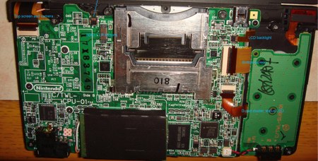
[bunnie] managed to pick up a Nintendo DSi while in Japan. It seems he had the device running less than an hour before he tore it down for an impromptu hotel photoshoot. There’s nothing too surprising and he mentions that the CPU certainly feels more capable than the previous model, which may explain the shorter battery life. The ARM processor sits under an RF shield directly below the WiFi card. The best photo is the top side of the board with every single debug point labeled in plain English on the silkscreen. We’re sure that’ll help with the development of new homebrew hardware.
[bunnie] has posted some interesting teardowns in the past. Have a look at his Sony XEL-1 teardown to see the inner workings of an OLED TV.
http://hackaday.com/2008/11/08/nintendo-dsi-teardown/
-
November 9th, 2008, 21:10 #2DCEmu Rookie

- Join Date
- Mar 2007
- Location
- York, UK
- Posts
- 174
- Rep Power
- 68


Hopefully the processor is more powerful, there's hope for the dsi!

 Reply With Quote
Thread Information
Users Browsing this Thread
There are currently 1 users browsing this thread. (0 members and 1 guests)

Bookmarks